NovaSilicon proposes CDK and compares analog-layout and digital-floorplanning agents
Two NovaSilicon papers report results on forty analog-layout tasks and one industrial floorplan, comparing general models, specialized systems and human references. The limited evaluations do not replace tape-out validation or prove an industry-wide Designless shift.
Editorial correction (November 16, 2026): The two team evaluations cover limited tasks and one industrial design. They do not replace tape-out validation or guarantee an industry-wide shift to Designless.
TSMC, founded in 1987, does only foundry work. A foundry packages its manufacturing processes into a PDK (Process Design Kit) and provides it to customers. The PDK embodies the foundry's core technology, shared with chip companies through limited interfaces while the core manufacturing recipes are retained. By using PDKs, chip companies can outsource manufacturing and concentrate on design themselves. Companies of this kind are called fabless.
Could the division of labor change again within design?
NovaSilicon, Shanghai Xinxingyuan Intelligent Technology, calls its approach CDK, Circuit Design Kit. It packages design experience and agents into a system. NovaSilicon engineers use it for iterative implementation between chip specifications and GDS layouts. The company says it first proposed CDK and calls the resulting division Designless: many design houses would shift away from maintaining their own design teams.
In two papers recently released around CDK, the company put the two agent systems within CDK and general-purpose agents such as GPT-6 Astra through the same set of problems. These included analog layout design and digital-chip floorplanning.
Its systems achieved the highest averages in both: 0.8154 for analog layout versus Astra’s 0.7483, and 57.97 for floorplanning, about 1.9 times Astra.
Within five months of founding, NovaSilicon raised hundreds of millions of yuan in three rounds. The latest was led by Shunwei Capital with GGV Capital and Matrix Partners China. Earlier investors included 5Y Capital, SenseTime Guoxiang Capital, Shanghai Future Industry Fund and Shanghai Science and Technology Innovation Group.
It has quickly recruited and trained engineers and researchers with both AI and chip-design expertise.
CDK: a PDK for design
NovaSilicon aims to repeat in design what foundries did in manufacturing. Agents and simulators are production equipment; CDK is the recipe. Specifications go in; GDS comes out.
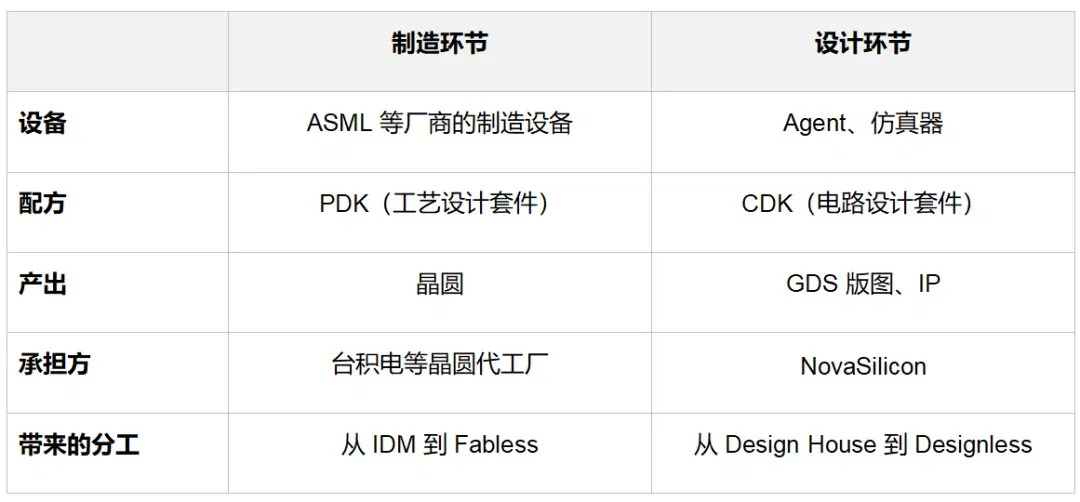
Table 1 | Comparing PDK and CDK. Source: NovaSilicon.
Designless follows Fabless specialization. Chip companies define specifications while CDK and its engineers implement them. NovaSilicon positions CDK as a model-driven AI–IC system, with design experience embedded in the kit rather than the model or EDA tool.
Analog CDK Vega covers topology, netlist-to-schematic conversion, sizing, simulation and layout. Digital CDK Sirius includes back-end initialization, floorplanning, placement/routing, clock trees, physical verification and timing, plus front-end specifications, modeling, RTL generation and verification.
Each paper tests one component: Vega’s Novara for analog layout and Sirius’s Nova-SI for floorplanning.
- Paper 1: AnalogLayoutWorld: An Open Benchmark for Agentic Analog Layout Design
- Paper 2: Evaluating AI Agents for Industrial-Level Chip Floorplanning: A Framework and Empirical Study
- Authors: Nova-Silicon Team
- Papers: [https://arxiv.org/abs/2611.12048, https://arxiv.org/abs/2611.16991]
General agents in analog layout: 91.1% submitted, 21.3% accepted
The first benchmark is AnalogLayoutWorld.
Layout is the final step in analog chip design. Circuit engineers first establish a transistor-level netlist, effectively a wiring table specifying which devices are used, how large they are and how they connect to one another. Layout engineers then follow it to draw the construction plan: turning each device into geometric shapes on silicon, positioning them, connecting the metal wires, and producing a GDS file that can be handed to the foundry.
AnalogLayoutWorld has 40 tasks covering amplifiers, reference sources, power-management circuits, sampling circuits and oscillators. Agents receive a fixed netlist and electrical specifications with which to perform layout design. Scoring considers six items: whether a GDS file is delivered; LVS, or whether the layout is consistent with the netlist; DRC, or whether process rules such as line widths and spacing are satisfied; area compactness; engineering quality; and whether post-layout simulation meets the targets. Engineering quality is defined jointly by the team and analog layout engineers, and examines such factors as device matching, critical-signal routing and power delivery.
Acceptance additionally requires all DRC, LVS and post-simulation conditions plus acceptable aspect ratio and shape.
Thirteen general-model/harness combinations and CDK Novara ran the same tasks.
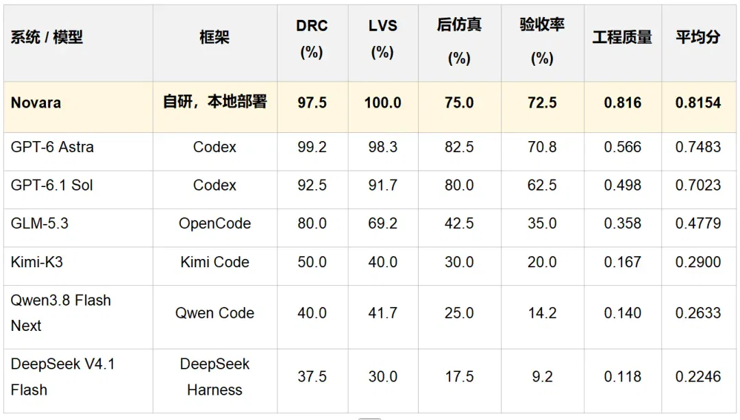
Table 2 | Selected AnalogLayoutWorld results. Source: paper Table 1.
Novara ranked first with a 0.8154 average and 72.5% acceptance. Astra scored 0.7483 with 70.8% acceptance; GPT-6.1 Sol scored 0.7023 and 62.5%. Two GLM-5.3 configurations averaged 0.46–0.48; all remaining configurations scored below 0.30.
Novara passed LVS in 100% of cases. Its engineering-quality score was 0.816 versus runner-up Astra’s 0.566.
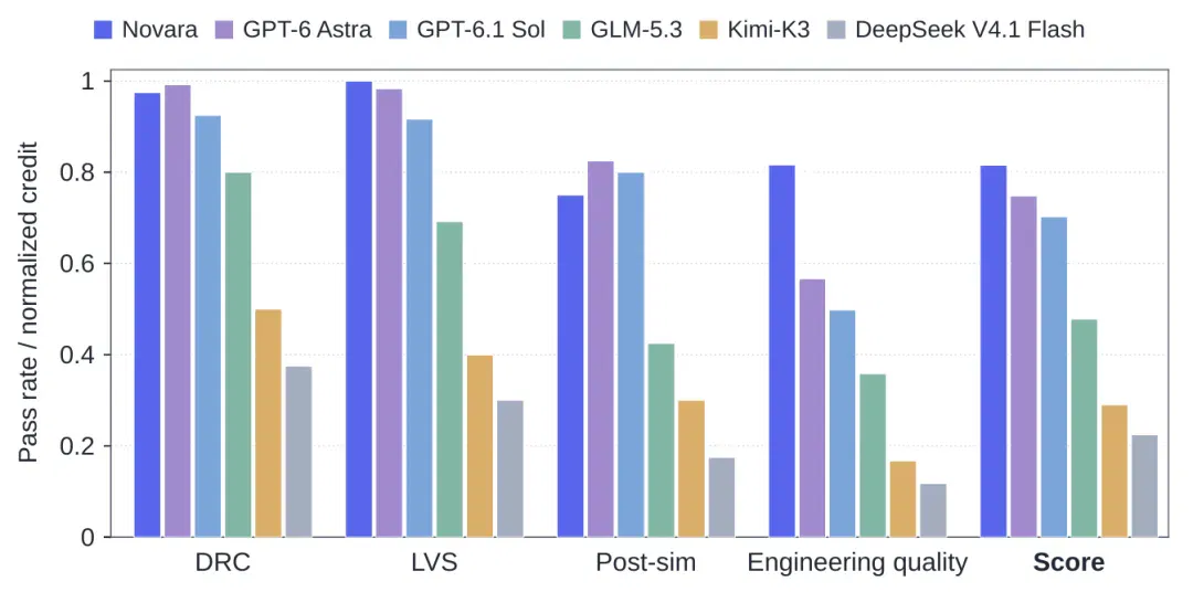
Figure 1 | Novara versus five general-agent configurations. DRC, LVS and Post-sim are pass rates; Score averages forty tasks. Source: paper.
Astra’s post-simulation pass rate of 82.5% exceeded Novara’s 75.0%, yet acceptance was only 70.8%. The paper attributes the loss mainly to aspect-ratio and shape failures. Novara’s 75.0% became 72.5%, so most simulation-passing layouts were accepted.
All simulations passed, but GPT delivered a 209-micrometer strip
A current-starved ring VCO task illustrates this. Astra passed DRC, LVS and both simulations in three attempts, but layouts were about 209 µm wide and under ten high, with aspect ratios 22.63–26.31 against a limit of four. Such strips are hard to integrate with neighboring circuits; all scored 0.3.
According to the trajectory logs, Astra first tried folding a long resistor in the circuit, but the folded design failed the length-parameter matching in LVS. It therefore reverted to a straight resistor 203.19 µm long and arranged the other devices in a line along it. This is a typical example of pursuing hard metrics while neglecting the requirements of actual analog-circuit tape-out.
Novara’s first attempt was 34.14 × 42.33 µm, aspect ratio 1.24, scoring 0.9015. Modeling engineers’ practical layout principles produced a more usable result.
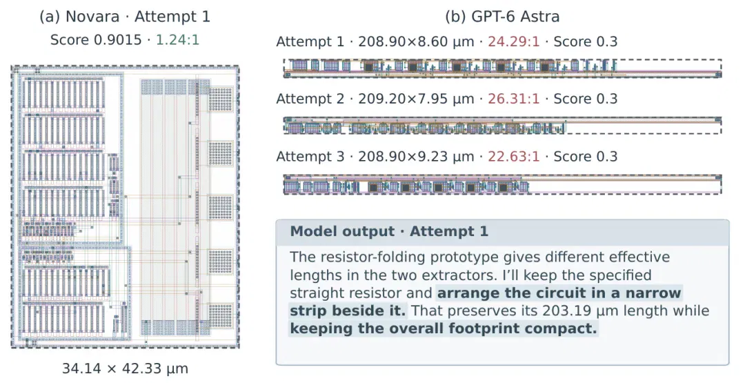
Figure 2 | Four ring-VCO layouts: Novara’s first on the left, Astra’s three on the right. All pass DRC, LVS and post-simulation. Source: paper.
One industrial design with 99 hard macros: about 1.9 times Astra’s average
The second paper tests digital back-end floorplanning.
The first step in turning a digital chip's logic netlist into a physical layout is deciding where the large modules should go. These large modules are called hard macros: their shapes are fixed and cannot be scaled. After the hard macros have been placed, EDA tools fill the remaining space with standard cells and connect the wiring. Intuitively, it is like first deciding where to put dozens of large buildings on a plot of land, leaving the rest for small houses and roads. If the buildings are poorly placed, local roads can still become congested even when the total area is sufficient.
The industrial design contains 235,727 instances. Ninety-nine macros occupy 71.1% of its 14.123 mm² L-shaped region, whose missing corner is unusable. Largest and smallest macro areas differ about 121-fold.
The evaluation connects the hard-macro placement submitted by an agent to a prescribed downstream flow: building the power and ground network, placing standard cells, estimating global routing and analyzing setup timing. The total evaluation score is out of 100 and is obtained by multiplying four components: congestion, timing, wire length and standard-cell utilization. The participating systems are divided into three groups. The first is Nova-SI, developed in-house by NovaSilicon and deployed locally. The second consists of general-purpose engineering agents that can query the design database, call EDA tools, receive feedback from the downstream flow and then make revisions. The third has only file read and write permissions.
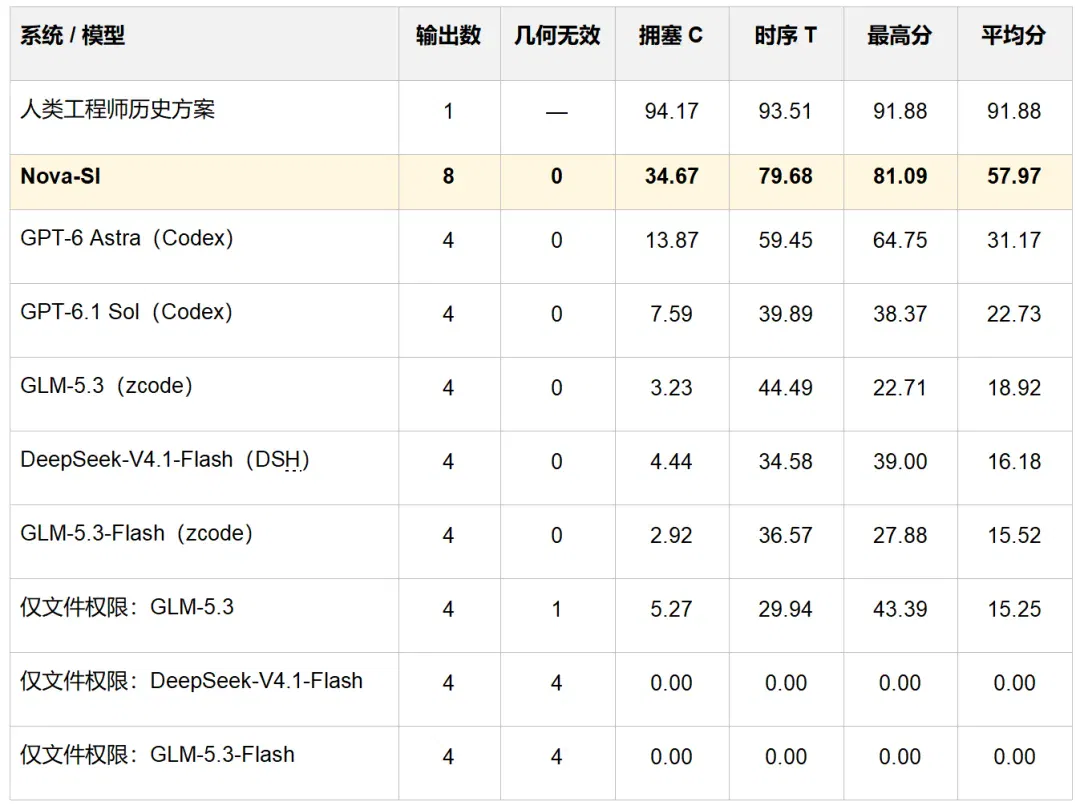
Table 3 | Floorplanning results. Scores are out of a hundred; invalid geometry or failed delivery scores zero. Source: paper Table 1.
Nova-SI averaged 57.97, Astra 31.17 and other general configurations fifteen to twenty-three. Nine of twelve file-only outputs overlapped or crossed boundaries and scored zero. All eight Nova-SI outputs passed geometry checks, with median 57.52 versus Astra’s 21.37. Three of four Astra outputs fell below Nova-SI’s worst. Nova-SI did not use online feedback from the prescribed flow, while general agents could inspect and revise with EDA. Average token use was 36.13M per Nova-SI output versus 62.11M–286.50M across five general configurations.
Removing Nova-SI’s best output leaves a 54.67 average. Scaling seven scoring parameters by 0.5, one or two yielded 2,187 combinations; its average remained 22.30–30.38 points above Astra. Its best score was 81.09; the historical human-engineered reference scored 91.88.
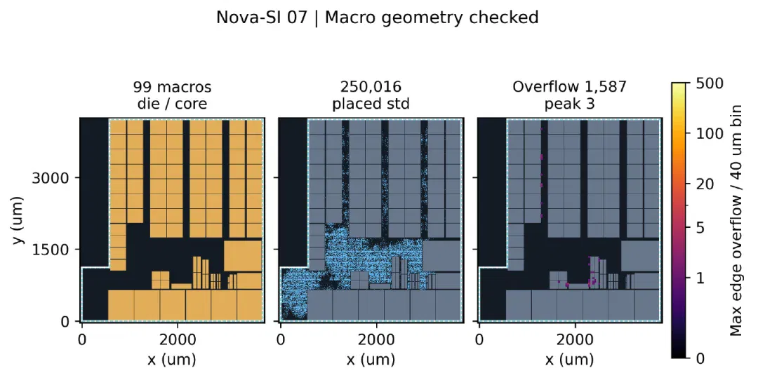
Figure 3 | Nova-SI’s best layout, number 07, score 81.09: macros, standard cells and congestion heatmap from left to right. Source: paper.
CDK’s future
CDK is first used in NovaSilicon's own design flow. Based on CDK, NovaSilicon currently serves chip design companies and customers with IP needs. There are two initial directions. One is UCIe PHY IP being developed using Vega. UCIe is an industry standard for chiplet interconnects, and PHY is its physical-layer interface. The other is design services for 3D compute-in-memory (CIM) chips, and the digital-design CDK, Sirius, is already being used in this service.
NovaSilicon hopes to change design-service specialization. Current results support further work in tested components; broad industry impact still depends on complete engineering validation, delivery and customer adoption.
DesignKit integration is a long-term direction, but scaling speed and returns remain unverified. The vision is not an established new scaling law.
This article was originally published by Synced. Author: Synced.
Related topics
After reading
Join the AINRK community
Read how to join the community and connect with people working in AI.
Related articles
Continue reading related topics and articles in this category.
ConvexLLM connects speech to language models through frozen text embeddings (opens in a new tab)
Researchers at CUHK-Shenzhen and Microsoft propose C-Gate, mapping audio into convex combinations of frozen text embeddings. The paper reports VoiceBench gains against its listed open-model baselines, while audio understanding and transcription still involve trade-offs.
CWM2.0 open-sources generative rendering with a 30-minute racing demo (opens in a new tab)
Teams from Ant, Westlake University and Zhejiang University use a structured Proxy to control scene state and Invoker-Render to generate visuals, releasing eight-GPU streaming inference. The long demo and 140 evaluations cover specified scenes, not arbitrary stable worlds.

Ankole outlines multi-user agent architecture: events, permissions and organizational memory (opens in a new tab)
The team describes its Business Harness design for fast and slow paths, shared state, Actor orchestration and dynamic permissions. Formal verification covers the modeled core permission state machine; it does not replace security checks of the full deployment, external interfaces or implementation.

openJiuwen presents a Harnessless approach for reusing AgentOS execution tools (opens in a new tab)
openJiuwen uses app-development and swarm demos to show how built-in harness capabilities support sessions, tools and app management. Applications still define business rules and permissions; remote deployment and some capabilities remain planned or exploratory.
Ask-to-Distill optimizes training questions using teacher–student distribution signals (opens in a new tab)
UIUC and collaborators propose A2D, training a question generator with frozen teacher–student disagreement and compatibility signals before on-policy distillation. The paper reports gains in math, code and agent tasks; its learning-value proxy has limits.